How Does VLSI Design Paves the Way for Advancement in IoT Appliances
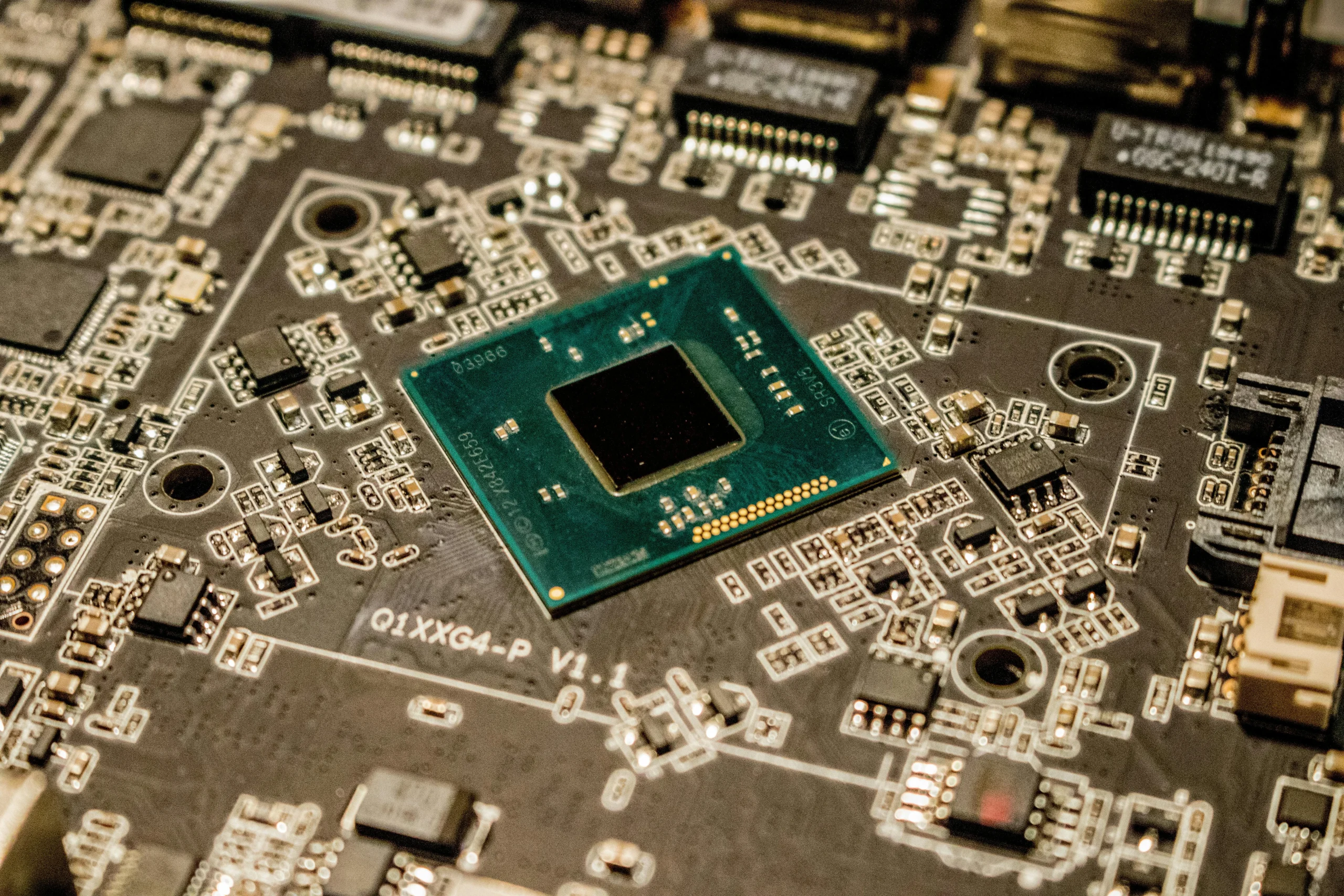
The industry of the technology realm is changing, and the Internet of Things is at the centre of transforming how we interact with machines and other gadgets. To facilitate the transformation process through the development of electronics that can be assimilated into almost every facet of life, the heart of vlsi layout, the vast field of Very Large Scale Integration of ICs, has become instrumental. VLSI design refers to the process of creating ICs with millions or billions of transistors, using organised creativity and the most efficient chip-making process, to strengthen the weak and modest feature manufacturers. The small but powerful ICs are the reason the Internet of Things has exploded, with IoT devices becoming more and more pervasive in our daily lives.
Contents
Miniaturisation
The reduction of electronic components to micrometre lengths is one of the specialties of VLSI design. With the help of sophisticated fabrication methods, VLSI engineers can design complex circuits that can be placed on one piece, making ultra-compact IoT devices possible. In addition to enabling a more subtle and attractive design, miniaturisation also makes it possible to implant electronics into normal occurrences. This function further blurs the barrier between the physical and digital worlds.
Think of a smartwatch that not just records your exercises but checks your critical signs as well as supplies real-time wellness insights. Or a clever home system that connects with every single device and component, enabling you to regulate and also automate almost every facet of your living environment from a single tool. These optimizations are feasible simply as a result of the VLSI layout’s miniaturisation.
Low power consumption
Power consumption is one of the most critical challenges when developing IoT devices. Considering that multiple appliances are run by batteries or low-power sources, energy efficiency is highly demanded. Here, VLSI design becomes a key pillar of solutions, as it allows for building ultra-low-power circuits. New techniques, such as clock gating, power gating, and dynamic voltage scaling, empower VLSI engineers to cut power consumption from IoT devices, making them consume fewer batteries, and be more environment-friendly.
A smart thermostat that can last for several years on a battery charge, or a wireless sensor network that can track the environmental conditions without new batteries. These and many more designs are made possible by the power-efficient possibilities of VLSI. The vlsi circuit design can be made small to consume minimal power. As a result, VLSI is the most effective option for designs that need to last as long as the battery charges or work in remote areas. Therefore, VLSI is still growing, and there will be plenty of more energy-efficient solutions to come.
Increased functionality
With the development of IoT devices, the requirements for their functionality also increase. VLSI design allows manufacturers to integrate a huge amount of analytical computation, memory, and specialised hardware into a single chip. In the future, it allows the devices to perform quite complex tasks – for example, real-time data analysis, or certain types of machine learning, as well as advanced signal processing, while remaining small-sized.
Visualise a smart home assistant that controls not just your lights and plugs but also listens to your verbal orders, predicts your reaction to your Google search inquiries, and, with time, comes to know your choices. This document will also outline a fitness LCD tracking time watch that measures and analyses physical exercise, sleeping, and physiology through information entered automatically. These intricate functions are made feasible by the high density of VLSI integration.
Security and privacy
Given the rising trend of IoT devices, the area of data security and privacy is becoming particularly relevant. VLSI design can help address the issue by allowing the integration of security features at the level of hardware to the chip directly. It includes but is not limited to hardware encryption, secure boot, and trusted execution environments all of which can assist in securing the data and preventing access or tampering.
Think of a home security system that is intelligent enough to safeguard your premises and encrypt and secure your data at the hardware layer, thereby guaranteeing your privacy and serenity. Similarly, no one would be able to reveal your health information if your wearable medical device could safeguard your data in the event of a violation. Through these and many other important measures, VLSI design provides critical security assurances that these IoT devices can be trusted with our most crucial data.
Scalability and adaptability
The world of IoT is without a doubt continuously advancing and growing. To stay aware of the most recent advancements, VLSI needs to stay adaptable and versatile. VLSI engineers should utilise a combination of modular design techniques and reconfigurable hardware design, allowing devices to be altered or improved to meet new requirements and needs.
Picture a smart home hub that adds new IoT devices as soon as they become available, for example, without requiring a new integrated circuit at the cost of hundreds of dollars. Or a wearable fitness monitor that is enhanced with new algorithms and sensors to stay ahead of the curve for the next few years. VLSI design accomplishes this versatility and scalability, which prolongs sensor nodes’ duration of relevance.
Artificial intelligence and machine learning
Artificial intelligence and machine learning capabilities will be increasingly required as IoT devices become more advanced. VLSI design is critical for creating such capabilities!, as it enables the integration of custom hardware accelerators and even dedicated neural processing units directly onto the chip. Hardware accelerators can dramatically improve the performance and energy efficiency of AI and ML workloads, allowing them to be processed and acted upon in real-time directly on the device.
Imagine a smart home assistant that becomes familiar with you and your home and creates customised recommendations and automated actions without needing to contact the cloud. Imagine a small wearable body camera that recognizes objects, people’s faces, and scenes in real time to improve user interactions and facilitate new solutions. This is not fantasy, but rather advanced AI and ML capabilities powered by VLSI design create a future for adaptable and intelligent IoT equipment.
Conclusion
As the IoT revolution continues to progress, VLSI design for embedded electronics design will become an essential tool for shaping the future of connected devices and appliances. VLSI design allows the miniaturisation of electronic components, low power consumption, improved functionality, high-level security, scalability, sensor integration, AI/ML, and smartphone capabilities, which leads to more advanced, efficient and intelligent IoT solutions.